Unijunction transistor (abbreviated as UJT), also called the double-base diode is a 2-layer, 3-terminal solid-state (silicon) switching device. The device has-a unique characteristic that when it is triggered, its emitter current increases re generatively (due to negative resistance characteristic) until it is restricted by emitter power supply. Since the device has one pn junction and three leads it is commonly called UJT.
1. Construction of a UJT
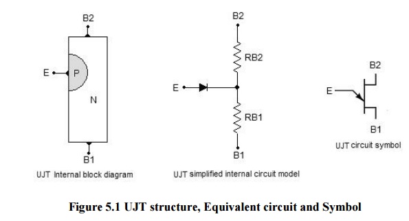
The basic structure of a unijunction transistor is shown in figure. It essentially consists of a lightly-doped N-type silicon bar with a small piece of heavily doped P-type material alloyed to its one side to produce single P-N junction. The single P-N junction accounts for the terminology unijunction. The silicon bar, at its ends, has two ohmic contacts designated as base-1 (B1) and base-2 (B2), as shown and the P-type region is termed the emitter (E). The emitter junction is usually located closer to base-2 (B2) than base-1 (B1) so that the device is not symmetrical, because symmetrical unit does not provide optimum electrical characteristics for most of the applications.
The symbol for unijunction transistor is shown in figure. The emitter leg is drawn at an angle to the vertical line representing the N-type material slab and the arrowhead points in the direction of conventional current when the device is forward-biased, active or in the conducting state. The basic arrangement for the UJT is shown in figure.
A complementary UJT is formed by diffusing an N-type emitter terminal on a P-type base. Except for the polarities of voltage and current, the characteristics of a complementary UJT are exactly the same as those of a conventional UJT.
The device has only one junction, so it is called the unijunction device.
The device, because of one P-N junction, is quite similar to a diode but it differs from an ordinary diode as it has three terminals.
The structure of a UJT is quite similar to that of an N-channel JFET. The main difference is that P-type (gate) material surrounds the N-type (channel) material in case of JFET and the gate surface of the JFET is much larger than emitter junction of UJT.
In a unijunction transistor the emitter is heavily doped while the N-region is lightly doped, so the resistance between the base terminals is relatively high, typically 4 to 10 kilo Ohm when the emitter is open.
The N-type silicon bar has a high resistance and the resistance between emitter and base-1 is larger than that between emitter and base-2. It is because emitter is closer to base-2 than base-1.
UJT is operated with emitter junction forward- biased while the JFET is normally operated with the gate junction reverse-biased.
UJT does not have ability to amplify but it has the ability to control a large ac power with a small signal. It exhibits a negative resistance characteristic and so it can be employed as an oscillator.
2. UJT parameters
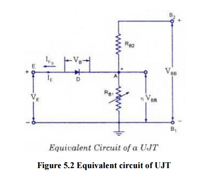
RBBO : It is the resistance between the terminals B1 and B2. In simple words, it is the resistance of the N-Type bar when measured lengthwise. If RB1is resistance of the bar from E to B1 and RB2 is the resistance of the bar from E to B2, then RBBO can be expressed as RBBO= RB1
+RB2. The typical range of RBBO is from 4KΩ to 10KΩ.
Intrinsic standoff ratio (η) : It is the ratio of RB1 to the sum of RB1 and RB2. It can be expressed as η = RB1/(RB1+RB2) or η = RB1/RBBO. The typical range of intrinsic standoff ratio is from 0.4 to 0.8
Operation of a UJT
Imagine that the emitter supply voltage is turned down to zero. Then the intrinsic stand-off voltage reverse-biases the emitter diode, as mentioned above. If VB is the barrier voltage of the emitter diode, then the total reverse bias voltage is VA + VB = η VBB + VB. For silicon VB = 0.7 V.
Now let the emitter supply voltage VE be slowly increased. When VE becomes equal to η VBB, IEo will be reduced to zero. With equal voltage levels on each side of the diode, neither reverse nor forward current will flow.
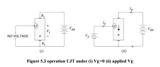
When emitter supply voltage is further increased, the diode becomes forward-biased as soon as it exceeds the total reverse bias voltage (ηVBB + VB). This value of emitter voltage VE is called the peak-point voltage and is denoted by VP. When VE = VP, emitter current IE starts to flow through RB1 to ground, that is B1. This is the minimum current that is required to trigger the UJT. This is called the peak-point emitter current and denoted by IP. Ip is inversely proportional to the interbase voltage, VBB.
Now when the emitter diode starts conducting, charge carriers are injected into the RB region of the bar. Since the resistance of a semiconductor material depends upon doping, the resistance of region RB decreases rapidly due to additional charge carriers (holes). With this decrease in resistance, the voltage drop across RB also decrease, cause the emitter diode to be more heavily forward biased. This, in turn, results in larger forward current, and consequently more charge carriers are injected causing still further reduction in the resistance of the RB region. Thus the emitter current goes on increasing until it is limited by the emitter power supply. Since VA decreases with the increase in emitter current, the UJT is said to have negative resistance characteristic. It is seen that the base-2 (B2) is used only for applying external voltage VBB across it. Terminals E and B1 are the active terminals. UJT is usually triggered into conduction by applying a suitable positive pulse to the emitter. It can be turned off by applying a negative trigger pulse.
UJT Characteristics
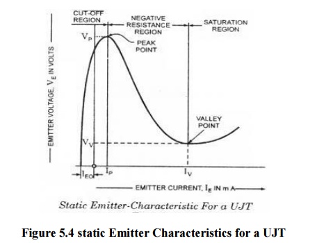
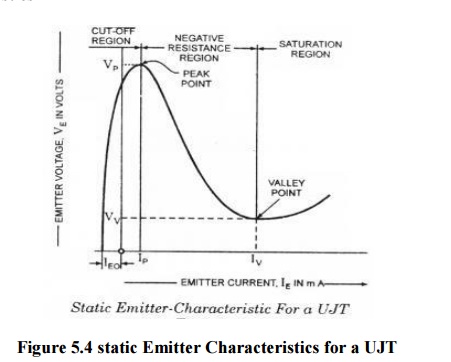
The static emitter characteristic (a curve showing the relation between emitter voltage VE and emitter current IE) of a UJT at a given inter base voltage VBB is shown in figure. From figure it is noted that for emitter potentials to the left of peak point, emitter current IE never exceeds IEo . The current IEo corresponds very closely to the reverse leakage current ICo of the
conventional BJT. This region, as shown in the figure, is called the cut-off region. Once conduction is established at VE = VP the emitter potential VEstarts decreasing with the increase in emitter current IE. This Corresponds exactly with the decrease in resistance RB for increasing current IE. This device, therefore, has a negative resistance region which is stable enough to be used with a great deal of reliability in the areas of applications listed earlier. Eventually, the valley point reaches, and any further increase in emitter current IE places the device in the saturation region, as shown in the figure5.4.
Three other important parameters for the UJT are IP, VV and IV and are defined below:
Peak-Point Emitter Current Ip : It is the emitter current at the peak point. It represents the rnimrnum current that is required to trigger the device (UJT). It is inversely proportional to the interbase voltage VBB.
Valley Point Voltage VV: The valley point voltage is the emitter voltage at the valley point. The valley voltage increases with the increase in interbase voltage VBB.
Valley Point Current IV: The valley point current is the emitter current at the valley point. It increases with the increase in inter-base voltage VBB.
Ø Special Features of UJT.
The special features of a UJT are :
1. A stable triggering voltage (VP)— a fixed fraction of applied inter base voltage VBB.
2. A very low value of triggering current.
3. A high pulse current capability.
4. A negative resistance characteristic.
5. Low cost.
3. Applications of UJT.
ü Relaxation oscillators.
ü Switching Thyristors like SCR, TRIAC etc.
ü Magnetic flux sensors.
ü Voltage or current limiting circuit.
ü Bistable oscillators.
ü Voltage or current regulators.
ü Phase control circuits.
Ø UJT relaxation oscillator.
The circuit diagram of a UJT relaxation oscillator is given shown above. R1 and R2 are current limiting resistors. Resistor R and capacitor C determines the frequency of the oscillator.
The frequency of the UJT relaxation oscillator can be expressed by the equation
F = 1/ (RC ln(1/(1-η))
Where η is the intrinsic standoff ratio and ln stand for natural logarithm.
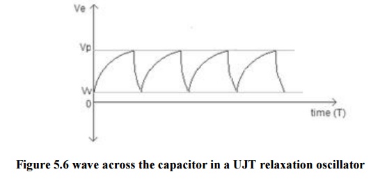
When power supply is switched ON the capacitor C starts charging through resistor R. The capacitor keeps on charging until the voltage across it becomes equal to 0.7V plus ηVBB. This voltage is the peak voltage point ―Vp‖ denoted in the characteristics curve (Fig:2). After this point the emitter to RB1 resistance drops drastically and the capacitor starts discharging through this path. When the capacitor is discharged to the valley point voltage ―Vv‖ (refer Fig : 1) the emitter to RB1 resistance climbs again and the capacitor starts charging. This cycle is repeated and results in a sort of sawtooth waveform across the capacitor. The saw tooth waveform across the capacitor of a typical UJT relaxation oscillator is shown in the figure below.
