A light emitting diode (LED) is known to be one of the best optoelectronic devices out of the lot. The device is capable of emitting a fairly narrow bandwidth of visible or invisible light when its internal diode junction attains a forward electric current or voltage.
The visible lights that an LED emits are usually orange, red, yellow, or green. The invisible light includes the infrared light. The biggest advantage of this device is its high power to light conversion efficiency. That is, the efficiency is almost 50 times greater than a simple tungsten lamp.
The response time of the LED is also known to be very fast in the range of 0.1 microseconds when compared with 100 milliseconds for a tungsten lamp. Due to these advantages, the device wide applications as visual indicators and as dancing light displays.
We know that a P-N junction can connect the absorbed light energy into its proportional electric current. The same process is reversed here. That is, the P-N junction emits light when energy is applied on it. This phenomenon is generally called electro luminance, which can be defined as the emission of light from a semi-conductor under the influence of an electric field.
The charge carriers recombine in a forward P-N junction as the electrons cross from the N-region and recombine with the holes existing in the P-region. Free electrons are in the conduction band of energy levels, while holes are in the valence energy band.
Thus the energy level of the holes will be lesser than the energy levels of the electrons. Some part of the energy must be dissipated in order to recombine the electrons and the holes. This energy is emitted in the form of heat and light.
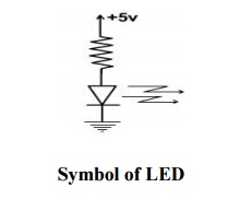
LED Circuit Symbol

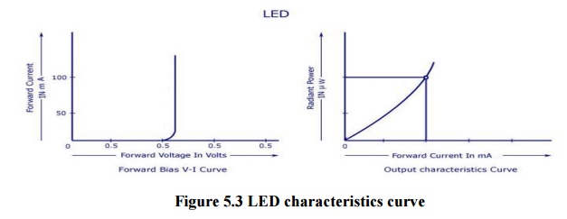
1. LED Characteristics

The forward bias Voltage-Current (V-I) curve and the output characteristics curve is shown in the figure above. The V-I curve is practically applicable in burglar alarms. Forward bias of approximately 1 volt is needed to give significant forward current. The second figure is used to represent a radiant power-forward current curve. The output power produced is very small and thus the efficiency in electrical-to-radiant energy conversion is very less.
The commercially used LED‘s have a typical voltage drop between 1.5 Volt to 2.5 Volt or current between 10 to 50 milliamperes. The exact voltage drop depends on the LED current, colour, tolerance, and so on.
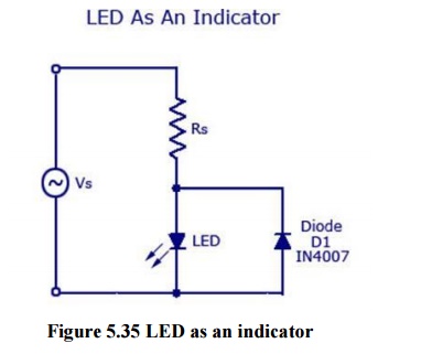
2. LED as an Indicator
The circuit shown below is one of the main applications of LED. The circuit is designed by wiring it in inverse parallel with a normal diode, to prevent the device from being reverse biased. The value of the series resistance should be half, relative to that o f a DC circuit.

LEDS displays are made to display numbers from segments. One such design is the seven-segment display as shown below. Any desired numerals from 0-9 can be displayed by passing current through the correct segments. To connect such segment a common anode or common cathode cathode configuration can be used. Both the connections are shown below. The LED‘s are switched ON and OFF by using transistors.
Ø Advantages of LED’s
· Very low voltage and current are enough to drive the LED.
· Voltage range – 1 to 2 volts.
· Current – 5 to 20 mill amperes.
· Total power output will be less than 150 mill watts.
· The response time is very less – only about 10 nanoseconds.
· The device does not need any heating and warm up time.
· Miniature in size and hence light weight.
· Have a rugged construction and hence can withstand shock and vibrations.
· An LED has a life span of more than 20 years.
Ø Disadvantages of LED
· A slight excess in voltage or current can damage the device.
· The device is known to have a much wider bandwidth compared to the laser.
· The temperature depends on the radiant output power and wavelength.

