Rectifiers are classified according to the period of conduction.
They are
Ø Half Wave Rectifier
Ø Full Wave Rectifier
FULL WAVE RECTIFIER
Full wave rectifier rectifies the full cycle in the waveform i.e. it rectifies both the positive and negative cycles in the waveform. We have already seen the characteristics and working of Half Wave Rectifier. This Full wave rectifier has an advantage over the half wave i.e. it has average output higher than that of half wave rectifier. The number of AC components in the output is less than that of the input.
The full wave rectifier can be further divided mainly into following types.
1. Center Tapped Full Wave Rectifier
2. Full Wave Bridge Rectifier
1. Centre-Tap Full Wave Rectifier
We have already discussed the Full Wave Bridge Rectifier, which uses four diodes, arranged as a bridge, to convert the input alternating current (AC) in both half cycles to direct current (DC).
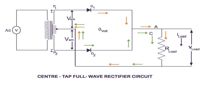
In the case of centre-tap full wave rectifier, only two diodes are used, and are connected to the opposite ends of a centre-tapped secondary transformer as shown in the figure below. The centre-tap is usually considered as the ground point or the zero voltage reference point.
· Working of Centre-Tap Full Wave Rectifier
As shown in the figure, an ac input is applied to the primary coils of the transformer. This input makes the secondary ends P1 and P2 become positive and negative alternately. For the positive half of the ac signal, the secondary point D1 is positive, GND point will have zero volt and P2 will be negative. At this instant diode D1 will be forward biased and diode D2 will be reverse biased. As explained in the Theory Behind P-N Junction and Characteristics of P-N Junction Diode, the diode D1 will conduct and D2 will not conduct during during the positive half cycle. Thus the current flow will be in the direction P1-D1-C-A-B-GND. Thus, the positive half cycle appears across the load resistance RLOAD.
During the negative half cycle, the secondary ends P1 becomes negative and P2 becomes positive. At this instant, the diode D1 will be negative and D2 will be positive with the zero reference point being the ground, GND. Thus, the diode D2 will be forward biased and D1 will be reverse biased. The diode D2 will conduct and D1 will not conduct during the negative half cycle. The current flow will be in the direction P2-D2-C-A-B-GND.
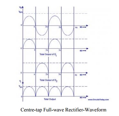
When comparing the current flow in the positive and negative half cycles, we can conclude that the direction of the current flow is the same (through load resistance RLOAD). When compared to the Half-Wave Rectifier, both the half cycles are used to produce the corresponding output. The frequency of the rectified output voltage is twice the input frequency. The output that is rectified, consists of a dc component and a lot of ac components of minute amplitudes.
Ø Peak Inverse Voltage (PIV) of Centre-Tap Full Wave Rectifier
PIV is the maximum possible voltage across a diode during its reverse biased period. Let us analyze the PIV of the centre-tapped rectifier from the circuit diagram. During the first half or the positive half of th input ac supply, the diode D1 is positive and thus conducts and provided no resistance at all. Thus, the whole of voltage Vs developed in the upper-half of the ac supply is provided to the load resistance RLOAD. Similar is the case of diode D2 for the lower half of the transformer secondary.
Therefore, PIV of D2 = Vm + Vm = 2Vm
PIV of D1 = 2Vm
Centre-Tap Rectifier Circuit Analysis
Ø Peak Current
The instantaneous value of the voltage applied to the rectifier can be written as
Vs = Vsm Sinwt
Assuming that the diode has a forward resistance of RFWD ohms and a reverse resistance equal to infinity, the current flowing through the load resistance RLOAD is given as
Im = Vsm/(RF + RLoad)
Ø Output Current
Since the current is the same through the load resistance RL in the two halves of the ac cycle, magnitude od dc current Idc, which is equal to the average value of ac current, can be obtained by integrating the current i1 between 0 and pi or current i2 between pi and 2pi.

Output current of centre Tap rectifier
Ø DC Output Voltage
Average or dc value of voltage across the load is given as

DC Output Voltage of centre Tap Rectifier
Ø Root Mean Square (RMS) Value of Current
RMS or effective value of current flowing through the load resistance RL is given as

RMS Value of Current of centre Tap Rectifier
Ø Root Mean Square (RMS) Value of Output Voltage
RMS value of voltage across the load is given as

RMS Value of Output Voltage of Centre Tap Rectifier
Ø Rectification Efficiency
Power delivered to load,
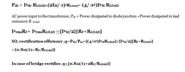
Rectification Efficiency of Centre Tap Rectifier
Ø Ripple Factor
Form factor of the rectified output voltage of a full wave rectifier is given as

Ripple Factor of centre Tap Rectifier
Ø Regulation
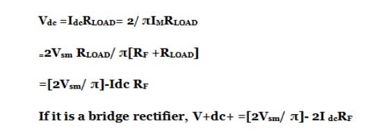
The dc output voltage is given as
2. Full wave bridge rectifier.
A Full wave rectifier is a circuit arrangement which makes use of both half cycles of input alternating current (AC) and convert them to direct current (DC). In our tutorial on Half wave rectifiers, we have seen that a half wave rectifier makes use of only one half cycle of the input alternating current. Thus a full wave rectifier is much more efficient (double+) than a half wave rectifier. This process of converting both half cycles of the input supply (alternating current) to direct current (DC) is termed full wave rectification.
Full wave rectifier can be constructed in 2 ways. The first method makes use of a center tapped transformer and 2 diodes. This arrangement is known as Center Tapped Full Wave Rectifier. The second method uses a normal transformer with 4 diodes arranged as a bridge. This arrangement is known as a Bridge Rectifier.
Full Wave Rectifier Theory
To understand full wave bridge rectifier theory perfectly, you need to learn half wave rectifier first. In the tutorial of half wave rectifier we have clearly explained the basic working of a rectifier. In addition we have also explained the theory behind a pn junction and the characteristics of a pn junction diode.
Full Wave Rectifier Working & Operation
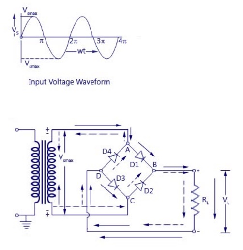
The working & operation of a full wave bridge rectifier is pretty simple. The circuit diagrams and wave forms we have given below will help you understand the operation of a bridge rectifier perfectly. In the circuit diagram, 4 diodes are arranged in the form of a bridge. The transformer secondary is connected to two diametrically opposite points of the bridge at points A & C. The load resistance RL is connected to bridge through points B and D.
· During the first half cycle
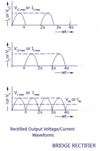
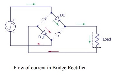
During first half cycle of the input voltage, the upper end of the transformer secondary winding is positive with respect to the lower end. Thus during the first half cycle diodes D1 and D3 are forward biased and current flows through arm AB, enters the load resistance RL, and returns back flowing through arm DC. During this half of each input cycle, the diodes D2 and D4 are reverse biased and current is not allowed to flow in arms AD and BC. The flow of current is indicated by solid arrows in the figure above. We have developed another diagram below to help you understand the current flow quickly. See the diagram below – the green arrows indicate beginning of current flow from source (transformer secondary) to the load resistance. The red arrows indicate return path of current from load resistance to the source, thus completing the circuit.
· During the second half cycle
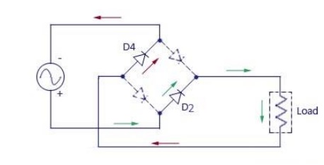
During second half cycle of the input voltage, the lower end of the transformer secondary winding is positive with respect to the upper end. Thus diodes D2 and D4 become forward biased and current flows through arm CB, enters the load resistance RL, and returns back to the source flowing through arm DA. Flow of current has been shown by dotted arrows in the figure. Thus the direction of flow of current through the load resistance RLremains the same during both half cycles of the input supply voltage. See the diagram below – the green arrows indicate beginning of current flow from source (transformer secondary) to the load resistance. The red arrows indicate return path of current from load resistance to the source, thus completing the circuit.
