PNP Transistor:
The integrated PNP transistors are fabricated in one of the following three structures.
1. Substrate or Vertical PNP
2. Lateral or horizontal PNP and
3. Triple diffused PNP
Substrate or Vertical PNP:
The P-substrate of the IC is used as the collector, the N-epitaxial layer is used as the base and the next P-diffusion is used as the emitter region of the PNP transistor. The structure of a vertical monolithic PNP transistor Q1 is shown in figure. The base region of an NPN transistor structure is formed in parallel with the emitter region of the PNP transistor.
The method of fabrication has the disadvantage of having its collector held at a fixed negative potential. This is due to the fact that the P-substrate of the IC is always held at a negative potential normally for providing good isolation between the circuit components and the substrate.
Triple diffused PNP:
This type of PNP transistor is formed by including an additional diffusion process over the standard NPN transistor processing steps. This is called a triple diffusion process, because it involves an additional diffusion of P-region in the second N-diffusion region of a NPN transistor. The structure of the triple diffused monolithic PNP transistor Q2 is also shown in the below figure.
This has the limitations of requiring additional fabrication steps and sophisticated fabrication assemblies.
Lateral or Horizontal PNP:
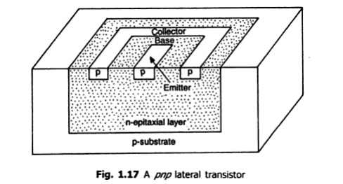
This is the most commonly used form of integrated PNP transistor fabrication method. This
has the advantage that it can be fabricated simultaneously with the processing steps of an NPN transistor and therefore it requires as the base of the PNP transistor. During the P-type base diffusion process of NPN transistor, two parallel P-regions are formed which make the emitter and collector regions of the horizontal PNP transistor.

Comparison of monolithic NPN and PNP transistor:
Normally, the NPN transistor is preferred in monolithic circuits due to the following reasons:
1. The vertical PNP transistor must have his collector held at a fixed negative voltage.
2. The lateral PNP transistor has very wide base region and has the limitation due to the lateral diffusion of P-type impurities into the N-type base region. This makes the photographic mask making, alignment and etching processes very difficult. This reduces the current gain of lateral PNP transistors as low as 1.5 to 30 as against 50 to 300 for a monolithic NPN transistor.
3. The collector region is formed prior to the formation of base and emitter diffusion. During the later diffusion steps, the collector impurities diffuse on either side of the defined collector junction. Since the N-type impurities have smaller diffusion constant compared to P-type impurities the N- type collector performs better than the P-type collector. This makes the NPN transistor preferable for monolithic fabrication due to the easier process control.
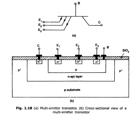
4. Transistor with multiple emitters: The applications such as transistor- transistor logic (TTL) require multiple emitters. The below figure shows the circuit sectional view of three N-emitter regions diffused in three places inside the P-type base. This arrangement saves the chip area and enhances the component density of the IC.


