
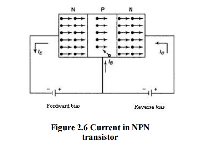
OPERATION OF AN NPN TRANSISTOR
Emitter base junction is forward biased and collector base junction is reverse biased. Due to emitter base junction is forward biased lot of electrons from emitter entering the base region.
Base is lightly doped with P-type impurity. So the number of holes in the base region is very small.
Due to this, electron- hole recombination is less (i.e,) few electrons(<5%) combine with holes to constitute base current(IB)
The remaining electrons (>95%) crossover into collector region, to constitute collector current(IC).
OPERATION OF A PNP TRANSISTOR
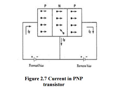
Emitter base junction is forward biased and collector base junction is reverse biased. Due to emitter base junction is forward biased lot of holes from emitter entering the base region and electrons from base to emitter region.
Base is lightly doped with N-type impurity. So the number of electrons in the base region is very small.
Due to this, electron- hole recombination is less (i.e,) few holes (<5%) combine with electrons to constitute base current(IB)