
The PAL device is a special case of PLA which has a programmable AND array and a fixed OR array. The basic structure of Rom is same as PLA. It is cheap compared to PLA as only the AND array is programmable. It is also easy to program a PAL compared to PLA as only AND must be programmed.
The figure 1 below shows a segment of an unprogrammed PAL. The input buffer with non inverted and inverted outputs is used, since each PAL must drive many AND Gates inputs. When the PAL is programmed, the fusible links (F1, F2, F3…F8) are selectively blown to leave the desired connections to the AND Gate inputs. Connections to the AND Gate inputs in a PAL are represented by Xs, as shown here:
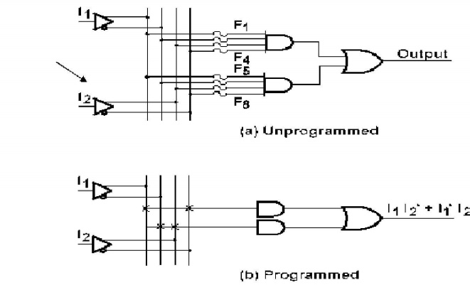
Figure 1: segment of an unprogrammed and programmed PAL.
As an example, we will use the PAL segment of figure 1 to realize the function I1I2‘+I1I2. theXs indicate that the I1 and I2‘ lines are connected to the first AND Gate, and the I1‘ and I2 lines are connected to the other Gate.
Typical combinational PAL have 10 to 20 inputs and from 2 to 10 outputs with 2to 8 AND gates driving each OR gate. PALs are also available which contain D flip-flops with inputs driven from the programming array logic. Such PAL provides a convenient way of realizing sequential networks. Figure 2 below shows a segment of a sequential PAL. The D flip-flop is driven from the OR gate, which is fed by two AND gates. The flip-flop output is fed back to the programmable AND array through a buffer. Thus the AND gate inputs can be connected to A, A‘, B, B‘, Q, or Q‘. The Xs on the diagram show the realization of the next-state equation.
Q+ = D = A‘BQ‘ + AB‘Q
The flip-flop output is connected to an inverting tristate buffer, which is enabled when
EN = 1
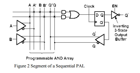
Figure 3 below shows a logic diagram for a typical sequential PAL, the 16R4.This PAL has an AND gate array with 16 input variables, and it has 4 D flip-flops. Eachflip-flop output goes through a tristate-inverting buffer (output pins 14-17). One input(pin 11) is used to enable these buffers. The rising edge of a common clock (pin 1) causesthe flip-flops to change the state. Each D flip-flop input is driven from an OR gate, andeach OR gate is fed from 8 AND gates. The AND gate inputs can come from the externalPAL inputs (pins2-9) or from the flip-flop outputs, which are fed back internally. Inaddition there are four input/output (i/o) terminals (pins 12,13,18 and 19), which can beused as either network outputs or as inputs to the AND gates. Thus each AND gate canhave a maximum of 16 inputs (8 external inputs, 4 inputs fed back from the flip-flopoutputs, and 4 inputs from the i/o terminals). When used as an output, each I/O terminalis driven from an inverting tristate buffer. Each of these buffers is fed from an OR gateand each OR gate is fed from 7 AND gates. An eighth AND gate is used to enable