PN JUNCTION DIODE
When the N and P-type semiconductor materials are first joined together a very large density gradient exists between both sides of the junction so some of the free electrons from the donor impurity atoms begin to migrate across this newly formed junction to fill up the holes in the P-type material producing negative ions.
1. FORWARD BIAS CONDITION
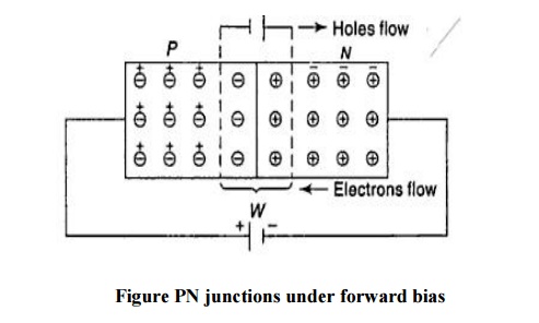
When positive terminal of the battery is connected to the P-type and negative terminal to N-type of the PN junction diode that is known as forward bias condition.
· Operation
The applied potential in external battery acts in opposition to the internal potential barrier which disturbs the equilibrium.
As soon as equilibrium is disturbed by the application of an external voltage, the Fermi level is no longer continuous across the junction.
Under the forward bias condition the applied positive potential repels the holes in P type region so that the holes move towards the junction and the applied positive potential repels the electrons in N type region so that the electrons move towards the junction.
When the applied potential is more than the internal barrier potential the depletion region and internal potential barrier disappear.

· V-I Characteristics
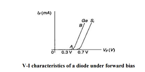
As the forward voltage increased for VF < Vo, the forward current IF almost zero because the potential barrier prevents the holes from P region and electrons from N region to flow across the depletion region in opposite direction.

For VF > Vo, the potential barrier at the junction completely disappears and hence, the holes cross the junction from P to N type and electrons cross the junction to opposite direction, resulting large current flow in external circuit.
A feature noted here is the cut in voltage or threshold voltage VF below which the current is very small. At this voltage the potential barrier is overcome and the current through the junction starts to increase rapidly.
· Cut in voltage is 0.3V for germanium and 0.7 for silicon.
2. UNDER REVERSE BIAS CONDITION
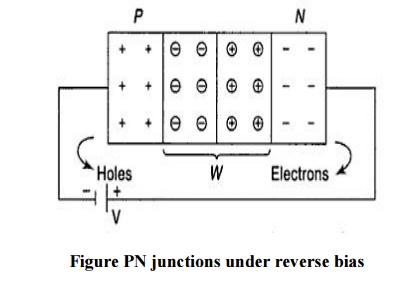
When the negative terminal of the battery is connected to the P-type and positive terminal to N-type of the PN junction diode that is known as forward bias condition.
· Operation
The holes from the majority carriers of the P side move towards the negative terminal of the battery and electrons which from the majority carrier of the N side are attracted towards the positive terminal of the battery.

Hence, the width of the depletion region which is depleted of mobile charge carriers increases. Thus, the electric field produced by applied reverse bias, is in the same direction as the electric field of the potential barrier.
Hence the resultant potential barrier is increased which prevents the flow of majority carriers in both directions. The depletion width W is proportional to under reverse bias.
· V-I characteristics
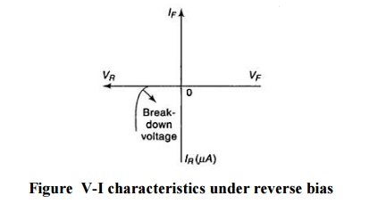
Theoretically no current flow in the external circuit. But in practice a very small amount of current of the order of few microamperes flows under reverse bias.

Electrons forming covalent bonds of semiconductor atoms in the P and N type regions may absorb sufficient energy from heat and light to cause breaking covalent bonds. So electron hole pairs continuously produced.
Consequently the minority carriers electrons in the P region and holes in the N region, wander over to the junction and flow towards their majority carrier side giving rise a small reverse current. This current is known as reverse saturation current Io.
The magnitude of this current is depends on the temperature because minority carrier is thermally broken covalent bonds.

