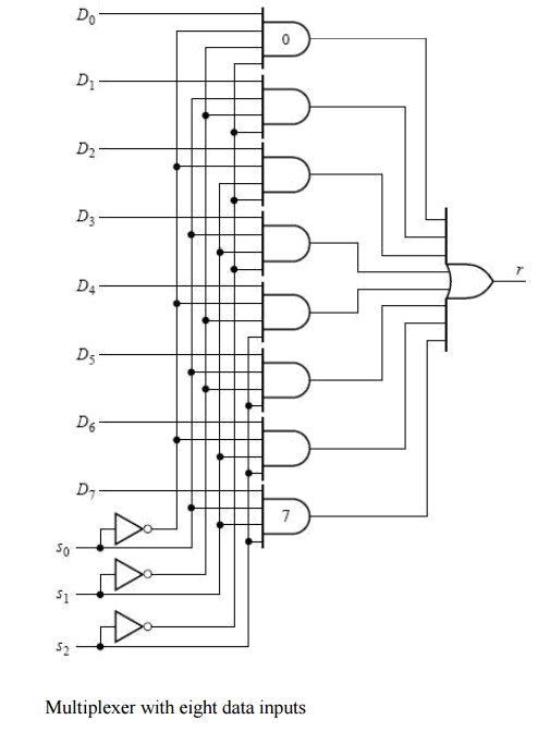
Many tasks in communications, control, and computer systems can be performed by combinational logic circuits. When a circuit has been designed to perform some task in one application, it often finds use in a different application as well. In this way, it acquires different names from its various uses. In this and the following sections, we will describe a number of such circuits and their uses. We will discuss their principles of operation, specifying their MSI or LSI implementations. One common task is illustrated in Figure 12. Data generated in one location is to be used in another location; A method is needed to transmit it from one location to another through some communications channel. The data is available, in parallel, on many different lines but must be transmitted over a single communications link. A mechanism is needed to select which of the many data lines to activate sequentially at any one time so that the data this line carries can be transmitted at that time.This process is called multiplexing.An example is the multiplexing of conversations on the telephone system. A number of telephone conversations are alternately switched onto the telephone line many times per second. Because of the nature of the human auditory system, listeners cannot detect that what they are hearing is chopped up and that other people‘s conversations are interspersed with their own in the transmission process.
Needed at the other end of the communications link is a device that will undo the multiplexing: a demultiplexer. Such a device must accept the incoming serial data and direct it in parallel to one of many output lines. The interspersed snatches of telephone conversations, for example, must be sent to the correct listeners.
A digital multiplexer is a circuit with 2n data input lines and one output line. It must also have a way of determining the specific data input line to be selected at any one time. This is done with n other input lines, called the select or selector inputs, whose function is to select one of the 2n data inputs for connection to the output. A circuit for n = 3 is shown in Figure 13. The n selector lines have 2n = 8 combinations of values that constitute binary select numbers

Multiplexers as General-Purpose Logic Circuits
It is clear from Figures 13 and 14 that the structure of a multiplexer is that of a two-level AND-OR logic circuit, with each AND gate having n + 1 inputs, where n is the number of select inputs. It appears that the multiplexer would constitute a canonic sum-of-products implementation of a switching function if all the data lines together represent just one switching variable (or its complement) and each of the select inputs represents a switching variable.
Let‘s work backward from a specified function of m switching variables for which we have written a canonic sum-of-products expression. The size of multiplexer needed (number of select inputs) is not evident. Suppose we choose a multiplexer that has m − 1 select inputs, leaving only one other variable to accommodate all the data inputs.We write an output function of these select inputs and the 2m–1 data inputs Di. Now we plan to assign m −1 of these variables to the select inputs; but how to make the assignment?4 There are really no restrictions, so it can be done arbitrarily. The next step is to write the multiplexer output after replacing the select inputs with m − 1 of the variables of the given function. By comparing the two expressions term by term, the Di inputs can be determined in terms of the remaining variable.

