
Transistorised Differential Amplifier
The transistorized differential amplifier basically uses the emitter biased circuits which are identical in characteristics. Such two identical emitter biased circuits are
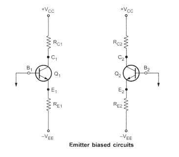
The two transistors Q1 and Q2 have exactly matched characteristics. The two collector Resistors R C1 and R C2 are equal while the two emitter resistances R E1 and R E2 are equal.
RC1 = RC2
And
RE1 = RE2
The magnitudes of + Vcc and – V EE are also same. The differential amplifier can be obtained by using such two emitter biased circuits. This is achieved by connectinemitter E1 of Q1 to the emitter E2 of Q2. Due to this, R E1 appears in parallel with R E2and the combination can be replaced by a single resistance denoted as R E. The base B1of Q1 is connected to the input 1 which is V S1 while the base B 2 of Q2 is connected to the input 2 which is Vs2. The supply voltages are measured with respect to ground. The balanced output is taken between the collector C1 of Q1 and the collector C2 of Q 2. Such an amplifier is called emitter coupled differential amplifier. The two collector resistances are same hence can be denoted as R C..
The output can be taken between two collectors or in between one of the two collectors and the ground. When the output is taken between the two collectors, none of them is grounded then it is called balanced output, double ended output or floating output. When the output is taken between any of the collectors and the ground, it is called unbalanced output or single ended output. The complete circuit diagram of such a basic dual input, balanced output differential amplifier is shown in the Fig.

As the output is taken between two output terminals, none of them is grounded, it is called balanced output differential amplifier.
Let us study the circuit operation in the two modes namely
i) Differential mode operation
ii)Common mode operation