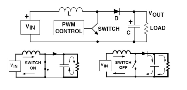
The Boost regulator takes a DC input voltage and produces a DC output voltage that is higher in value than the input (but of the same polarity). The Boost regulator is shown in Figure, along with details showing the path of current flow during the switch on and off time. Whenever theswitch is on, the input voltage is forced across the inductor which causes the current through it to increase (ramp up).

When the switch is off, the decreasing inductor current forces the "switch" end of the inductor to swing positive. This forward biases the diode, allowing the capacitor to charge up to a voltage that is higher than the input voltage. During steady-state operation, the inductor current flows into both the output capacitor and the load during the switch off time. When the switch is on, the loadcurrent is supplied only by the capacitor.
Output Current and Load power:
An important design consideration in the Boost regulator is that the output load current and the switch current are not equal, and the maximum available load current is always less than the current rating of the switch transistor. It should be noted that the maximum total power available for conversion in any regulator is equal to the input voltage multiplied times the maximum average input current (which is less than the current rating of the switch transistor). Since the output voltage of the Boost is higher than the input voltage, it follows that the output current must be lower than the input current.

